Image Gallery
Image Gallery
You are welcome to use our images for a class or presentation, please reference “Minot Group, Oregon State University”.
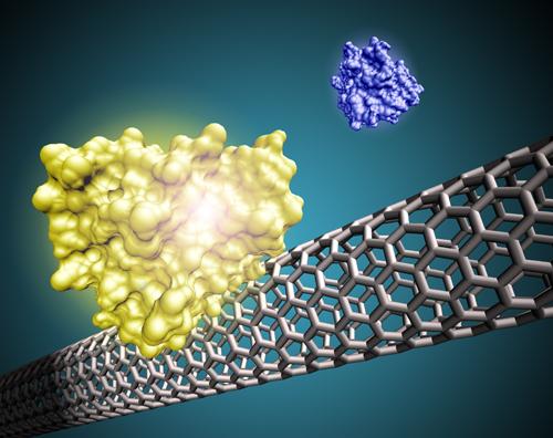
Proteins tumbling in solution can find their way to a carbon nanotube. Binding events modify the nanotube's resistance, a phenomena that can be used for electronic detection of biomolecules. Image by Landon Prisbrey.
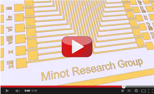
A fly-by tour of a carbon nanotube field-effect transistor chip. Amination by Tristan DeBorde.
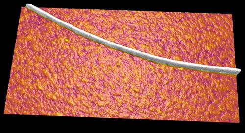
A carbon nanotube grown on a silicon oxide surface, imaged by atomic force microscopy. The scan size 400 x 800 nanometers.
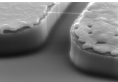
A suspended carbon nanotube bridging the gap between a pair of electrodes. The nanotube diameter is about 2 nanometers and it is hanging about 1 micron above the canyon floor. We use nanotubes in this geometry for a number of fundamental studies. Image by Tal Sharf.

We study the optoelectronic properties of suspended carbon nanotubes. The number is parentheses (26, 10) refer to the chiral index of the carbon nanotube. We don't control chiral index when we grow CNTs, instead, we determine chiral index after the CNT device is complete. Image by Tristan DeBorde.
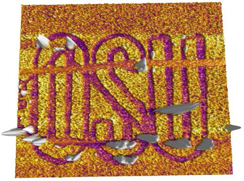
Proteins form a coating on glass surfaces. In this case, the protein coating is 4 nanometers thick. We scratched throught the protein layer using an atomic force microscope tip. By programming the motion of the tip, we created a very, very, very small university logo. Each letter is about the same size an e-coli bacteria. The total size of this image is 3 x 3 microns.
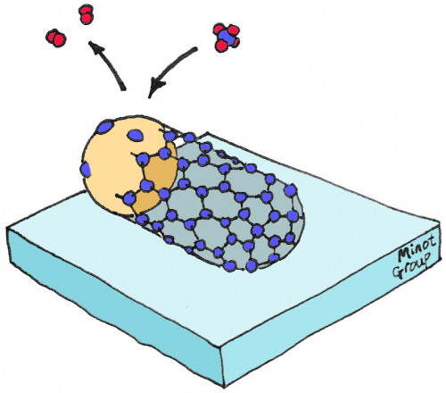
Cartoon drawing of the chemical vapor deposition process that we use to grow carbon nanotubes. The orange sphere is an iron nanoparticle, the surface underneth is silicon oxide. The chemical vapor deposition process is carried out at 900 degrees Celsius in the presence of methane and hydrogen gas.
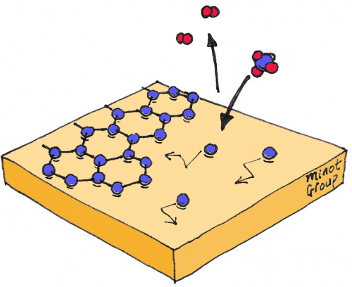
Cartoon drawing of the chemical vapor deposition process for graphene. The orange surface is copper foil. The process is carried out at 1000 degrees Celsius in the presence of methane and hydrogen gas.